


ASML debunks peak litho narrative
ASML’s High NA EUV technology is poised to follow the transformative path of Low NA EUV, enhancing efficiency and advancing chip design. This marks a promising trajectory for ASML's future growth.
ASML ($ASML) held their capital markets day (CMD or “Investor Day”) on November 14th, during which they reiterated their previous guidance to deliver annual revenues of between €44bn and €60bn by 2030, with a gross margin of between 56% and 60%. For comparison, the market currently expects 2024 revenues of €28 billion with a gross margin of approximately 51%.
As TSMC, Samsung, and others have been cautious with their wafer fabrication equipment (WFE) spending for the past two years, the idea of “peak litho” (“peak lithography”) has gained traction among some semiconductor commentators. However, ASML’s CMD last week appears to have debunked most of this narrative. In fact, 2025 could very well be the year TSMC begins ramping up its capital expenditure (CapEx) once again - directly impacting ASML’s system sales and bookings.
Economic Daily News reports that TSMC is accelerating its global expansion due to geopolitical factors, with plans for ten construction projects either ongoing or set to launch by 2025. The article highlights that this aggressive expansion will likely drive a significant rise in TSMC’s 2025 CapEx. The company’s previous record for annual capital expenditures was $36 billion in 2022. Their 2025 CapEx is said to possibly reach between $34 billion and $38 billion, potentially exceeding the previous peak.
TSMC itself has however clarified that it has not yet released detailed plans for its 2025 CapEx.
Yole Intelligence, a semiconductor market research firm, expects that the next WFE growth phase is approaching, as shown in Chart 1. below. I have previously written about the potential upcoming semiconductor CapEx supercycle, and I believe that Yole is too conservative in their CAGR forecast.

ASML’s system sales growth has experienced a minor bump in the road during 2024, as shown in Chart 2. below, but is posied for growth in 2025 and onwards as the next CapEx cycle likely begin.

In 2025, ASML will continue to deliver on its current EUV backlog (see Chart 3. below for the amount of ordered vs shipped EUV units since 2021) and likely experience renewed growth in EUV bookings for delivery in the 2026–2029 timeframe.

Advanced logic and DRAM in the spotlight
ASML made it clear that the semiconductor market is currently undergoing a significant transformation, with advanced logic and DRAM taking center stage, thus changing the overall market mix going forward. The company expects that EUV lithography spending will grow at a compound annual growth rate (CAGR) of 10–20% for logic and 15–25% for DRAM between 2025 and 2030, likely outpacing the growth of total WFE spending. In Figure 1. below (from ASML’s CMD), the amount of expected EUV exposures and EUV lithography spending growth is presented.

The company pointed out that achieving the full potential of AI requires substantial advancements in cost efficiency and energy consumption going forward, and that Extreme Ultraviolet (EUV) lithography is still poised to play a pivotal role in meeting these demands.
EUV increases efficiency and reduces cost
The EUV technology offers a proven path to significantly reduce both costs and energy consumption. For example, introducing EUV in high-bandwidth memory (HBM) production enables DRAM manufacturers to eliminate over 100 process steps - out of a total of approximately 700-750.
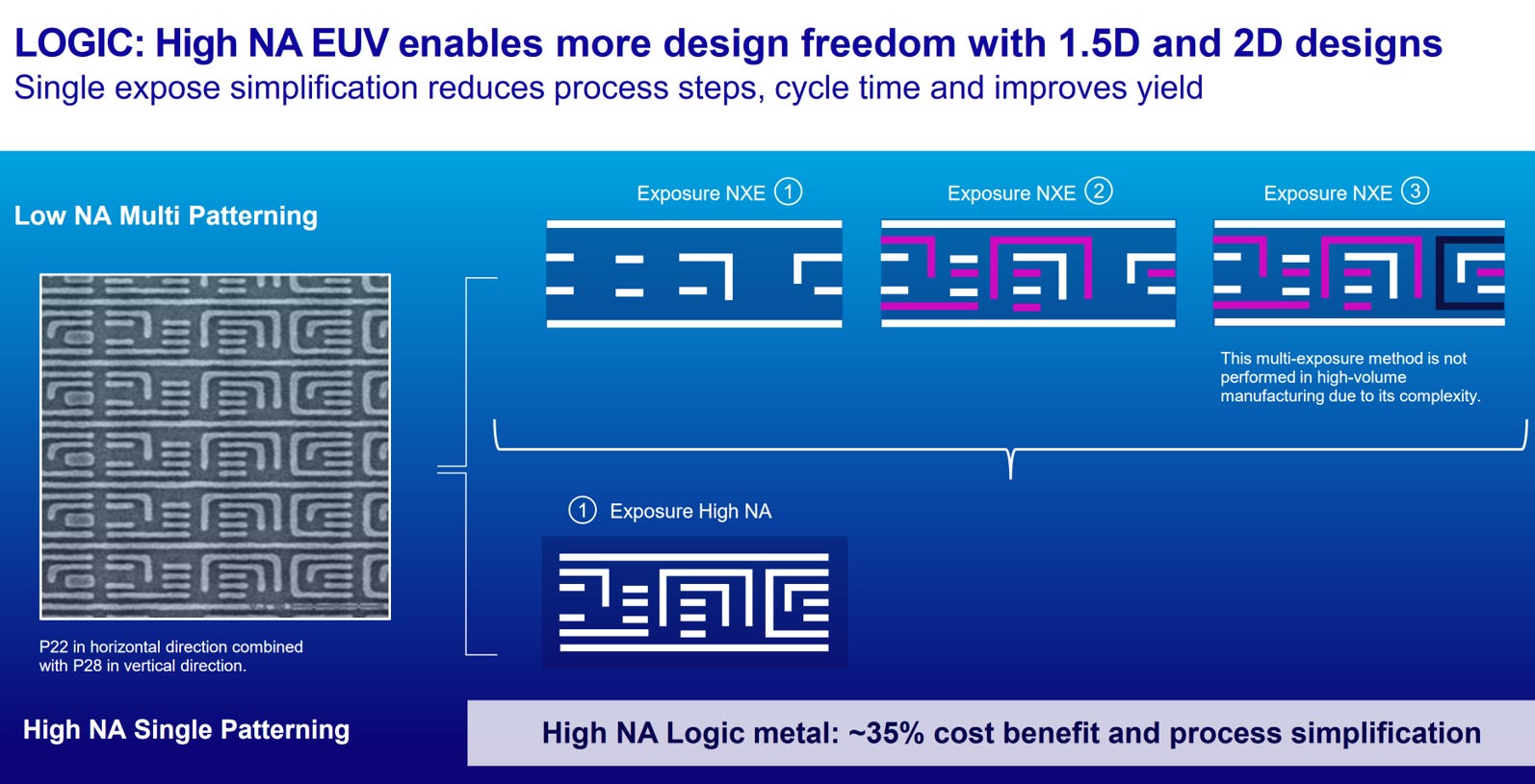
Although the pace of process shrinkage has slowed, it continues steadily in both logic and DRAM. The adoption of additional EUV layers remain as the most efficient way to achieve shrinkage, particularly for advanced logic nodes and DRAM. By reducing the reliance on multi-patterning (LE-LE-LE, or Litho Etch Litho Etch Litho Etch), EUV simplifies processes, lowers costs, and improves throughput. This is shown below, in Figure 2.

As new production processes (or nodes) get introduced, multi-patterning techniques (multiple exposures to create one layer) face physical limitations, particularly with immersion lithography (DUV). Since 2019, EUV has replaced a significant portion of DUV multi-patterning processes. Single-exposure EUV offers a simpler, faster, and more cost-effective solution. Furthermore, the shift from multi-patterning to single-exposure EUV layers is expected to accelerate over the coming years.
TSMC’s EUV adoption
To give readers a feeling for how the EUV adoption has developed over the years since 2019, the historical timeline for TSMC’s EUV adoption and layer/mask penetration is listed below. It provides a good indication of the general trend for EUV adoption:
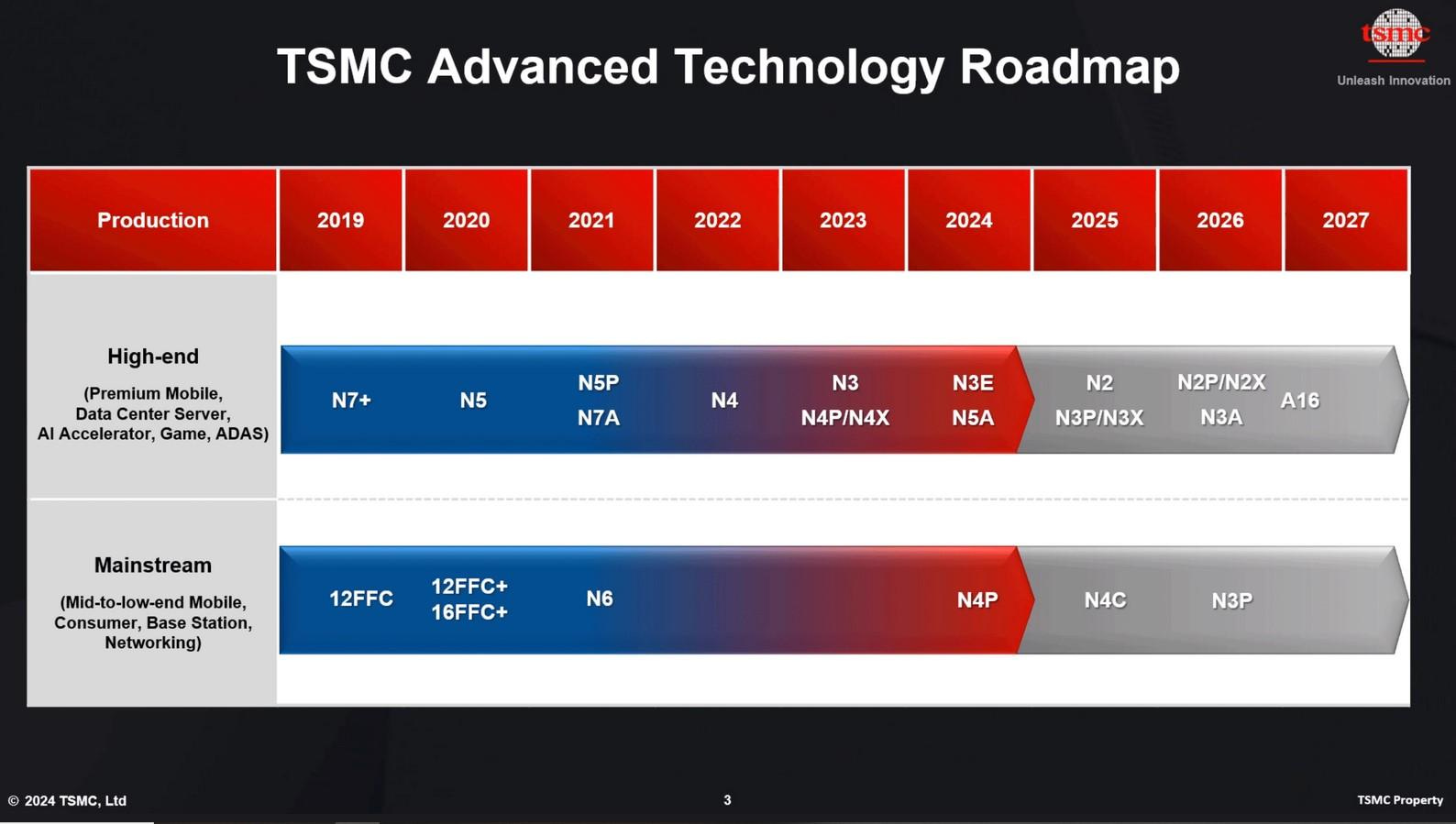
N7+ (7nm+):
Total layers: c80-85 (whereof c75-80 DUV layers)
First node to introduce EUV in production.
EUV is used for 4-5 layers (initial adoption). Replaced approximately 10-12 DUV exposures with EUV.
N6 (6nm):
Total layers: c80-85 (whereof c75-80 DUV layers).
EUV is used for up to 5 layers. Replaced roughly 10-12 DUV exposures.
N5 (5nm):
Total layers: c85 (whereof c50-55 DUV layers). Significant increase of EUV layers, enabling better transistor density and efficiency.
EUV is used for c14-15 layers and replaced around 30-40 DUV exposures.
Unpatterned layers: c15-20.
N4 (4nm):
Total layers: c85-90 (whereof c45-50 DUV layers). Small process improvements and slightly increased EUV use.
EUV is used for c14-16 layers. Replaced around 30-45 DUV exposures.
Unpatterned layers: c15-20.
N3 (3nm):
Total layers: c90 (whereof c30-40 DUV layers).
EUV is used for c20-25 layers, depending on specific design optimizations. Replaced approximately 50-60 DUV exposures.
Unpatterned layers: c15-20.
While TSMC has managed to optimize its EUV use on some nodes, it has not managed to fundamentally reduce the use of EUV - especially not between full node transitions. For instance, the original N3 (3nm) process involves approximately 25 EUV layers as listed above. However, with the introduction of derivative nodes such as N3E (an optimization of N3), TSMC has reduced the EUV layer count to 19 or 20 while improving process performance, power, and yield. For their next node, N2, the EUV layer count is expected to be 20+.
High NA EUV enters the chat
High NA EUV (High Numerical Aperture EUV) represents the next wave of lithography innovation from ASML, addressing the increasing complexity and cost of multi-patterning with low NA EUV.
High NA tools enable single-exposure patterning for advanced nodes, reducing mask counts by up to two-thirds and cutting costs by approximately 35%. It also provides chip designers greater flexibility by supporting two-dimensional designs, which improve device density and reduce the need for multiple interconnect layers. This is why ASML has been able to put a price tag of more than €400 million per High NA EUV tool.
Figure 4. and Figure 5. below show examples of how High NA will enable new design opportunities and reduced Low NA exposures.

As shown in Figure 6. below, ASML expects that by 2030, advanced logic will incorporate an average of 4–6 High NA EUV layers, while DRAM is projected to use 2–3 High NA layers. These advancements will significantly enhance productivity, reduce defect rates, and lower patterning costs.

Low NA EUV will in the meantime continue to replace DUV layers, while High NA EUV will start replacing Low NA EUV layers that would otherwise require multiple exposures. Does this signal a “peak lithography” moment? Hardly. Instead, it suggests that High NA EUV is poised to follow the same path that Low NA EUV once took, positioning ASML to sustain its growth trajectory once the current cyclical pause in WFE spending unpauses itself due to the laws of physics and surging costs.
EUV power and productivity innovations
EUV light sources have seen remarkable progress since 2019, with output power climbing from 200 watts to over 500 watts, and 700 watts demonstrated. Ongoing R&D suggests that power levels beyond a kilowatt are achievable. This innovation underpins EUV's scalability, enabling higher wafer throughput and better cost efficiency. For instance, High NA single-exposure productivity is projected to reach 300 wafers per hour, outperforming low NA double-exposure processes.


It’s a wrap
The above post shows that ASML is serious about pushing the boundries for chip designs and manufacturing, while at the same time keeping its firm grip around the industry’s capital expenditures. It will likely take more than a couple of years of CapEx consolidation before the industry's reliance on ASML (lithography) starts to decline.
I will end this article with a quote from lithos (@lithos_graphein) on X.com, a must-follow for anyone interested in ASML and lithography. The post highlights some of the groundbreaking, and impressive, technological advancements ASML continues to deliver and likely will deliver, to further enhance efficiency.